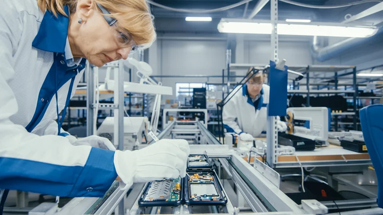
Manufacturers of PCBs for medical devices have become increasingly interested in yield enhancement and rework solutions in recent years. This interest is partly sparked by the fact that a typical PCB maker generates a huge amount of process and test data during test operations. The amount of data produced keeps increasing as automated inspection instrumentation advances. In addition, data accuracy is increasing as a result of the development of better defect or failure analysis tools. Rapid defect analysis and identification can be helpful since it can cut down on the reaction time, rework, and expenses associated with manufacturing and SMT Assembly issues.
Automated optical inspection is one of the main instruments used by contract PCB and electronics manufacturers (AOI). The appeal of the automatic systems can be better understood when compared to the efficiency and repeatability of human inspectors. For instance, an electronics contract manufacturer’s typical PCB assembly line employs two to four inspectors for an inspection and rework operation. An AOI system, on the other hand, just needs one operator to choose the programmes, find flaws, and fix faulty PCBs, significantly decreasing a company’s need for workers every shift. However, a factory should conduct a realistic assessment of all the elements that affect yield improvement and return on investment (ROI) before making an investment in automation.
BETTER TECHNOLOGY
Early in the 1980s, AOI systems were initially made available to the PCB assembly sector. These initial systems were expensive, slow, and challenging to programme. They were meant to replace human inspectors in the duty of evaluating PCBs for visual flaws like as missing pieces and layout problems.
New generations of AOI systems can now overcome these restrictions thanks to recent advancements in PC computing power, software, and image technologies. There are numerous locations along an assembly line where these technologies can be used in various ways. The inspection usually happens following part placement, reflow, or final assembly in surface-mount technology (SMT) scenarios.
An AOI system may detect a variety of flaws, including solder flaws, polarisation issues, missing parts, wrong components, and positioning errors. This entire list of defects has been identified and reported for rework. However, there are definite system restrictions. AOI systems perform great optical inspection of the board surface, but they can only detect characteristics that are visible to the naked eye. Chip-scale packages (CSPs), flip-chips, ball-grid arrays (BGAs), micro-BGAs, and other hidden-connection technologies require manufacturers to use x-ray technology to examine the essential solder joints. Additionally, double-sided PCBs need to be “flipped” for an accurate examination of both sides.


