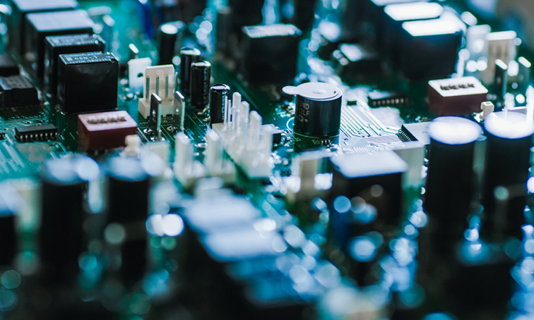
The steps of the PCB design process start with design and verification and continue through the fabrication of the circuit boards. Many steps require computer guidance and machine-driven tools to ensure accuracy and prevent short circuits or incomplete circuits.
Step One: Designing the PCB
Extended Gerber encodes all the information that the designer needs, such as the number of copper layers, the number of solder masks needed, and the other pieces of component notation.
Step Two: Design Review and Engineering Questions
Another key step of the printed circuit board fabrication process involves checking the design for potential errors or flaws.
Step Three: Printing the PCB Design
After all the checks are complete, the PCB design can be printed. A special kind of printer, known as a plotter printer, is used. A plotter printer makes a “film” of the PCB.
Step Four: Printing the Copper for the Interior Layers
Step four is the first step in the process where the manufacturer starts to make the PCB.
Step Five: Etch the Inner Layers or Core to Remove Copper
The core or inner layers of the PCB need to have extra copper removed before the PCB fabrication process can continue. Etching involves covering the necessary copper on the board and exposing the rest of the board to a chemical. The chemical etching process removes all unprotected copper from the PCB, leaving only the board’s necessary amount.
Step Six: Layer Alignment
After each of the PCB’s layers has been cleaned, they’re ready for layer alignment and optical inspection. The holes from earlier are used to align the inner and outer layers.
Step Seven: Automated Optical Inspection
Following the optical punch, another machine performs an optical inspection to make sure there are no defects.
Step Eight: Laminating the PCB Layers
At step six in the process, the PCB layers are all together, waiting to be laminated.
Step Nine: Drilling
Before drilling, an X-ray machine is used to locate the drill spots.
Step Ten: PCB Plating
After the panel has been drilled, it’s ready to be plated. The plating process uses a chemical to fuse all of the different layers of the PCB together.
Step Eleven: Outer Layer Imaging
Earlier in the process (Step Four), a photoresist was applied to the PCB panel. In Step Eleven, the photoresist is only applied to the outside layer, since it still needs to be imaged.
Step Twelve: Outer Layer Etching
When it comes time to etch the outside layer for the last time, the tin guard is used to help protect the copper during the etching process. Any unwanted copper is removed using the same copper solvent from earlier, with the tin protecting the valued copper of the etching area.
Steps Thirteen: Outer Layer AOI
As with the inner layer, the outer layer must also undergo automated optical inspection. This optical inspection ensures the layer meets the exact requirements of the design.
Step Fourteen: Solder Mask Application
Panels require a thorough cleaning before the solder mask application. Once clean, each panel has an ink epoxy and solder mask film covering the surface. Next, ultraviolet light strikes the boards to indicate where the solder mask needs removal.
Step Fifteen: Silkscreen Application
Because PCBs need to have information directly on the board, fabricators must print vital data on the surface of the board in a process referred to as silkscreen application or legend printing.
Step Sixteen: Finishing the PCB
Finishing the PCB requires plating with conductive materials.
Step Seventeen: Electrical Reliability Test
After the PCB has been coated and cured (if necessary), a technician performs a battery of electrical tests on the different areas of the PCB to ensure functionality.
Step Eighteen: Profiling and Route Out
Profiling requires fabrication engineers to identify the shape and size of the individually printed circuit boards cut from the construction board.
Step Nineteen: Quality Check and Visual Inspection
After scoring and breaking the boards apart, the PCB must undergo one final inspection before packaging and shipping.
Yeetek Electronics is one of the leading electronic components company. We are a trusted PCB board manufacturer all around the globe.
Also Read: How Software Can Make Your Business More Successful


